CD Laboratory for Advanced Computational Design of Crystal Growth (ACDC)
 infrastructure.")
This CD laboratory develops innovative modeling methods for the virtual description of crystal growth processes in the semiconductor industry. To this end, physics-based and data-driven modeling approaches are combined to achieve the most efficient and predictive approach possible.
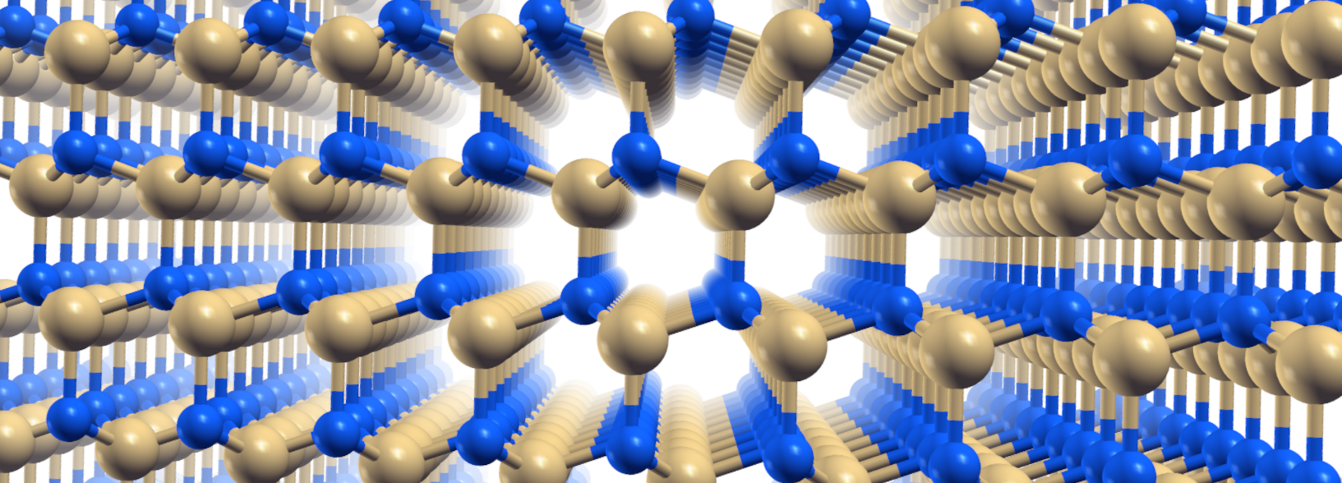
Semiconductors with a wide bandgap have enormous potential for future applications in power electronics, especially in the field of e-mobility: The laboratory focuses on silicon carbide, or SiC for short, which is particularly promising in this context. SiC-based components can be operated at higher voltages and temperatures than would be possible with silicon-based components. At the same time, switching frequencies can be increased and power losses reduced by up to half.
However, in order to enable the mass production of high-quality SiC crystals using physical vapor deposition, modeling methods are needed that are capable of predicting crystal growth processes as accurately as possible. In order to develop such methods, a central problem must first be solved: Physics-based models that are based on the latest knowledge of the physical processes of crystal growth, are already well advanced in principle, but must use approximations to perform the calculations. On the other hand, data-driven models could generate highly useful information for describing the growth of SiC crystals. However, these models are in turn limited by the current lack of “big data” in this area. Models of this type, as their name suggests, require a large amount of data and therefore require a corresponding number of experiments to be carried out – but these are extremely expensive, especially in the field of crystal growth.
The CD Laboratory for Computer-Aided Design of Crystal Growth Processes is therefore working to solve this problem by combining both types of models: so-called hybrid models are to be developed that combine physics-based and data-driven models in order to achieve the greatest predictive power. The aim is to work comprehensively and efficiently towards a method for optimally describing and predicting the growth processes of SiC crystals, which are particularly promising for the semiconductor industry, and to make this method transferable to other crystals in the future.

The furnaces for growing silicon carbide are simulated with multiphysics simulations to access relevant quantities such as magnetic fields, temperatures and mass transport. In experiments, these quantites are very difficult or even impossible to access.

